Headline & Intro
Intel is quietly trying to reinvent itself not in transistors, but in the "boring" part of the chip business that suddenly isn’t boring at all: advanced packaging. If this bet works, Intel can matter again in the AI race without instantly matching TSMC on the most advanced process nodes. If it fails, the company will have burned billions on another grand turnaround story. In this piece, we’ll look at what Intel is actually doing in New Mexico and Malaysia, why AI makes packaging strategic, how this changes the foundry game—and what it should signal to policymakers and customers in Europe.
The News in Brief
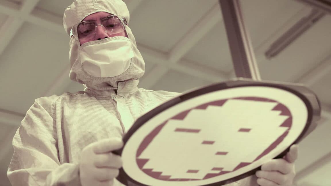
According to a report from Wired, syndicated by Ars Technica, Intel is pouring billions of dollars into advanced chip packaging facilities, with its Rio Rancho site in New Mexico at the center of the plan. A previously mothballed fab (Fab 9) was restarted in 2024 with support from the US CHIPS Act, and together with neighboring Fab 11X it now underpins Intel’s packaging push.
This activity sits inside Intel Foundry, the contract manufacturing arm that Intel has structurally separated from its traditional CPU product business. Intel executives told investors they expect packaging revenue to exceed US$1 billion and to arrive earlier than significant wafer revenue from the foundry side. The company has been in talks with large cloud providers—including, per Wired’s reporting, Google and Amazon—about using Intel for advanced packaging of their custom chips. Intel is also expanding assembly and test capacity with advanced packaging capabilities in Penang, Malaysia, as global AI demand drives interest in higher‑end packaging solutions such as its EMIB, Foveros and the upcoming EMIB‑T technologies.
Why This Matters
For years, the chip industry story was simple: whoever had the smallest transistors won. That is no longer true. In AI especially, the bottleneck is increasingly in how multiple chiplets, memory stacks and interconnects are packaged together rather than in any single die. This is precisely the layer Intel is trying to own.
If Intel can turn packaging into a real business line, several things change:
Intel gets back into the game without beating TSMC at 2 nm. The company has openly struggled to catch up at leading‑edge process nodes. Packaging is a flanking move: Intel can integrate dies from different vendors, mix process generations and still add value. That is far more realistic in the short term than outright process leadership.
Hyperscalers gain leverage. Google, Amazon and others are already designing their own AI chips. If they can shop wafers from one foundry and high‑end packaging from another, they are no longer fully captive to TSMC’s one‑stop model. Even the possibility of using Intel strengthens their negotiation position.
Margins are attractive. Intel’s CFO talks about 40% gross margins on packaging—similar to its traditional product business. With AI demand off the charts, premium packaging capacity is scarce and can command high prices.
Traditional OSATs get squeezed at the high end. Outsourced assembly and test providers like ASE and Amkor long dominated packaging. But the most advanced 2.5D/3D AI packaging is now being pulled in‑house by TSMC, Samsung—and potentially Intel. OSATs risk being pushed down to lower‑margin, less complex work.
The losers, at least in the short term, may be any customer who hopes that advanced packaging will quickly become a generic commodity. Intel’s bet is exactly the opposite: that leading‑edge packaging is scarce, expensive and strategically vital.
The Bigger Picture
Intel’s move fits three converging trends in semiconductors.
1. Chiplets and heterogeneous integration.
AMD popularised chiplet‑based CPUs with Ryzen and EPYC: multiple smaller dies connected on a package instead of one huge monolithic die. Apple links two M1 Max dies into an M1 Ultra. The industry is working on standards like UCIe to enable mixing dies from different vendors. All of this only works if packaging technology can provide high‑bandwidth, low‑latency, power‑efficient connections between these chiplets and stacked memories.
TSMC’s CoWoS and SoIC offerings already deliver this for Nvidia’s AI GPUs and many data‑center parts. Intel’s EMIB and Foveros were its answer; EMIB‑T is the next step, promising tighter connections and better power efficiency. In other words, packaging has become a performance feature, not just a cost line.
2. AI as a bandwidth and memory problem.
Training large AI models is less about raw compute and more about moving huge datasets between compute and high‑bandwidth memory (HBM). Recent GPU shortages were not only about chip wafers; CoWoS packaging capacity at TSMC was another bottleneck. Whoever controls advanced packaging effectively controls how much usable AI compute the market can deploy.
That is why Intel keeps repeating that packaging can be a "differentiator": if it can offer denser chip‑to‑chip links or more flexible configurations, hyperscalers can build AI systems tuned to their workloads, from huge training clusters to latency‑sensitive inference chips.
3. Geopolitics and supply‑chain resilience.
Front‑end manufacturing is heavily concentrated in Taiwan and South Korea. Back‑end assembly and packaging are mostly in Southeast Asia. The US, EU and others woke up to the geopolitical risk of this concentration. The US CHIPS Act funding for Rio Rancho is not just about jobs in New Mexico; it is about having at least part of the advanced packaging chain on US soil.
Intel’s Malaysia expansion shows that, realistically, no country is going to fully on‑shore everything soon. But it also underlines that back‑end is now recognized as strategic infrastructure in its own right—not a disposable afterthought.
The European / Regional Angle
From a European perspective, Intel’s packaging push is a warning shot and an opportunity.
The EU Chips Act has focused political messaging on front‑end fabs: Intel’s planned megafab in Magdeburg, TSMC’s plant in Dresden with European partners, and expansions by STMicroelectronics and GlobalFoundries. Packaging has received far less public attention, even though Europe relies heavily on Asian sites for advanced assembly of the very chips it designs and uses.
Intel’s strategy highlights that value and control are shifting into the package. If Europe ends up with shiny lithography‑heavy fabs but still sends wafers abroad for advanced AI packaging, it will remain strategically dependent—and vulnerable to the same bottlenecks that constrained Nvidia GPUs.
There are bright spots. Research hubs like imec in Belgium and Fraunhofer in Germany have world‑class expertise in 2.5D/3D integration. Intel has already invested heavily in Ireland; it has also discussed building an advanced packaging and assembly site in Italy, although details remain fluid. European cloud players—from OVHcloud to Deutsche Telekom and Orange—stand to benefit from more competition in AI‑class packaging, even if the capacity initially sits outside the EU.
But for policymakers in Brussels, Berlin, Paris and beyond, the message is clear: a serious semiconductor strategy needs to treat advanced packaging as a first‑class citizen. Otherwise, Europe risks subsidising wafers that will still be finished—and strategically controlled—elsewhere.
Looking Ahead
The next 24–36 months will determine whether Intel’s packaging pivot is remembered as a clever detour or another over‑promised turnaround.
What to watch:
Public hyperscaler wins. A confirmed Google or Amazon deal for EMIB/Foveros/EMIB‑T packaging would instantly validate Intel’s strategy. The first signs may show up not as press releases but as Intel Foundry’s capital‑expenditure spike and capacity expansions.
Execution and yield. 3D stacking and ultra‑fine interconnects are unforgiving. Intel’s recent history is full of slipped roadmaps. If EMIB‑T volume ramps on time, with competitive yields, it will signal that the company’s manufacturing culture really has changed.
TSMC’s response. TSMC is unlikely to watch calmly while key customers experiment with Intel packaging. The soft threat is allocation: in a world of tight supply, customers know that shifting part of the flow to a rival might one day influence how many wafers they get.
Regulatory attention. As packaging becomes a chokepoint, expect it to appear in export‑control debates and industrial policy. The same way advanced GPUs for AI ended up on export‑control lists, certain packaging configurations—especially those enabling huge HBM bandwidth—could come under scrutiny.
For customers, the opportunity is clear: more flexibility, potentially lower total system cost, and a route to differentiate beyond simply buying the latest off‑the‑shelf GPU. The risk is ending up tied to another single‑vendor dependency if Intel becomes the only realistic alternative to TSMC for the highest‑end AI packaging.
The Bottom Line
Intel has finally found a battleground where it isn’t obviously outgunned: advanced chip packaging at AI scale. If it can convert promising technology and government subsidies into real customer wins, packaging could become Intel’s fastest path back to strategic relevance—even without immediate process‑node supremacy. But this is also a reminder for Europe and for hyperscalers: in the AI era, power is shifting from the individual chip to how everything is stitched together. Are we investing as much thought—and money—into that layer as it deserves?


